Skip to content

News & Events

UW introduces virtual reality training for students to help fill crucial semiconductor jobs
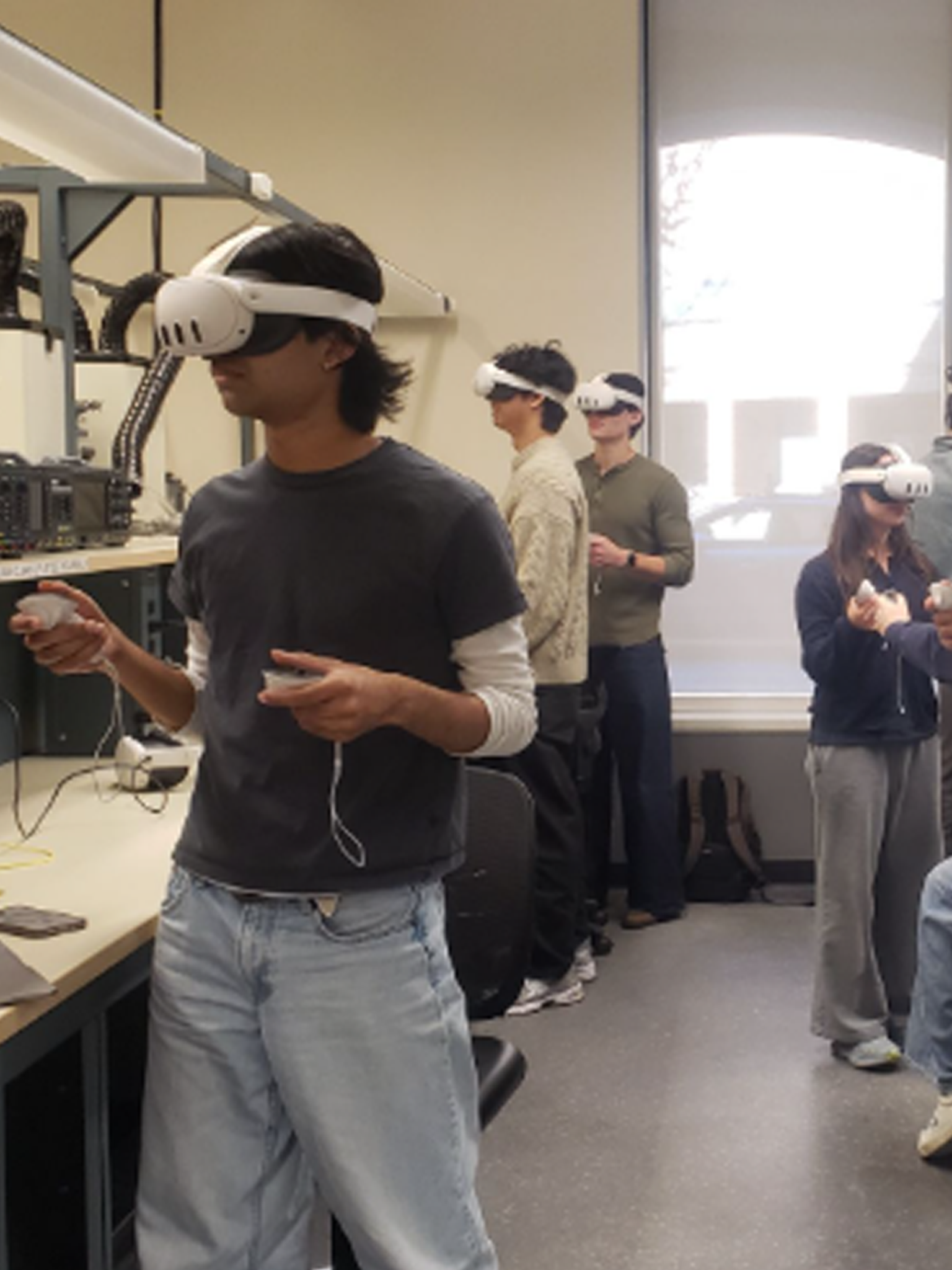
June 25, 2026 — A University of Washington course is using virtual reality modules to train students for in-demand semiconductor jobs. Electrical & Computer Engineering Associate Teaching Professor Tai-Chang Chen adopted the Cornell NanoScale Facility (CNF) Virtual Reality (VR) educational platform for his Devices and Circuits 1 (EE 331) course this spring to offer students the job skills needed to fill the growing semiconductor technical workforce gap. Semiconductor chips control electricity in just about every piece of modern technology. And since they are even smaller than microscopic airborne particles that can cause device failures, their production requires a controlled environment that only a cleanroom can provide.   Based on…

SEMI Foundation and NSF launch Regional Nodes of the National Network for Microelectronics Education

May 26, 2026: The SEMI Foundation — the Hub Operator for the National Network for Microelectronics Education (NNME) — launched four Regional Nodes of the NNME, each designed to prepare the next generation of America’s semiconductor design and manufacturing workforce. PINES (Pacific-Intermountain Network for Education in Semiconductors) has officially been selected as one of the Regional Nodes, which includes the Washington Nanofabrication Facility (WNF) at the University of Washington among its members. Led by Boise State University, the NNME Pacific…

UW research team creates a new type of optical chip

May 1, 2026: A research team led by Arka Majumdar, NanoES faculty member and UW Electrical & Computer Engineering (ECE) and Physics professor, has engineered a new type of optical microchip. This programmable photonic integrated circuit was fabricated in the Washington Nanofabrication Facility (WNF) and is low power, electrically reconfigurable, and can be mass-produced. Read more about this chip that has the potential to be applied in a wide range of technologies, including information processing, sensing, imaging, machine learning and…

How hands-on experience at WNF led a mechanical engineering student to Intel

April 29, 2025 — Four years ago, as an Engineering Dean’s Scholar, Jimmy Phan was listening to a lecture from the College of Engineering’s associate dean, Dan Ratner. Ratner told Phan’s cohort about the Washington Nanofabrication Facility (WNF), an open-access nanofabrication facility at the UW, and the opportunities for undergraduates to work there. By his second year of school, Phan was employed as an undergraduate lab assistant in the facility. Students working in the WNF have a unique opportunity to receive on-the-job training from…

Precision at the smallest scale

By Chelsea Yates Photos by University of Washington Step inside the Washington Nanofabrication Facility, where tiny tech is transforming research in quantum physics, chips, medicine and more. Imagine a high-tech workshop where scientists and engineers craft objects so small they can’t be seen with the naked eye — or even a standard microscope. These tiny structures — nanostructures — are thousands of times smaller than a strand of hair. And they are essential for faster computers, better smartphones and life-saving…

2025 NWNLA Workshop

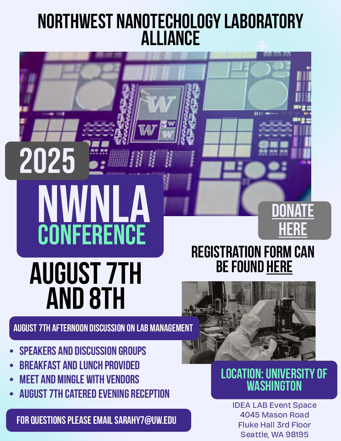
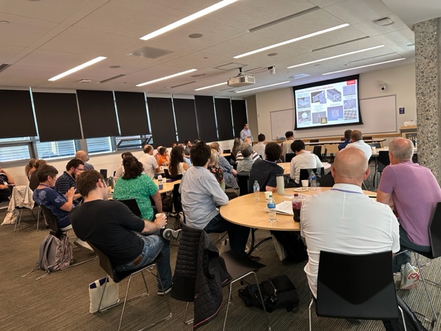
The Washington Nanofabrication Facility is excited to host the third meeting of the Northwest Nanotechnology Laboratory Alliance (NWNLA) at the University of Washington Seattle campus August 7th and 8th . Please view our save the date by clicking this link NWNLA 2025 Attendee Registration Form Vendor Registration Form           Hotel Recommendations  Watertown Hotel University Inn Silver Cloud Inn UW Campus housing options    

WNF student lands dream internship at Nvidia

Jan. 27, 2025 — In the University of Washington’s Washington Nanofabrication Facility (WNF), undergraduate lab assistants have a unique opportunity to receive on-the-job training from research engineers and network with professionals in advanced electronics, nanotechnology, semiconductors and fabrication-related jobs. Fourth-year electrical and computer engineering major Prithvi Krishnaswamy’s work in the WNF helped him land a summer internship at Nvidia, a company that designs hardware and software for the high-performance computing (HPC) market. Krishnaswamy interned at its Durham, North Carolina office. WNF:…

WNF director in working group targeting billions in CHIPS and Science Act funding for Washington state

Dec. 17. 2024 — Maria Huffman, director of the University of Washington’s Washington Nanofabrication Facility, is part of a new, state-wide group of leaders from universities, research institutions, technology companies and the government who aim to strengthen the state’s semiconductor industry. The group, organized by the Washington Department of Commerce, will work to attract federal funding through the CHIPS and Science Act.

Washington Nanofabrication Facility Updates

Nov. 27, 2023 — Scientists and engineers working in the Washington Nanofabrication Facility (WNF) have been busy over the past few months. In August, the WNF hosted the biannual Northwest Nanotechnology Laboratory Alliance (NWNLA) with generous support from Montana State University and the Molecular Analysis Facility. The goal of the biannual conference is to build partnerships between labs and foster community collaboration between lab users and vendors. This year, vendors and lab staff attended a variety of presentations, round table discussions,…

2025 NWNLA Workshop

The second meeting of the Northwest Nanotechnology Laboratory Alliance (NWNLA), a joint NNCI initiative between the Northwest Nanotechnology Infrastructure and the Montana Nanotechnology Facility, will be held in person at the UW in Seattle and virtually on August 8, 2025. This workshop is for staff and management of micro and nanofabrication facilities and imaging and analysis facilities from academia, industry, and government in the northwest.