WNF: What is your role at WNF?
Dr. Fred Newman: The short answer is I am focused on two process integration projects using a somewhat overlapping toolset, and I am responsible for some of the key tools in those areas in terms of training and maintenance.
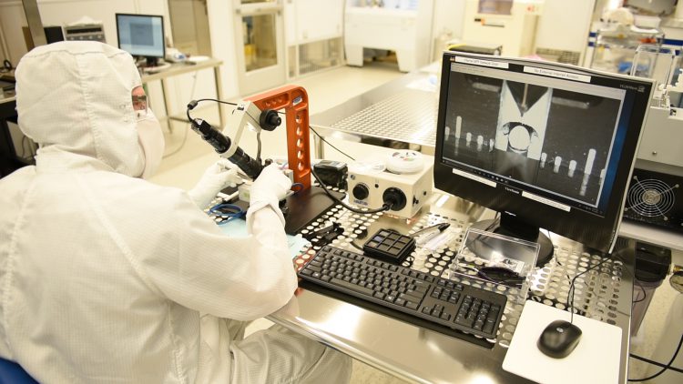
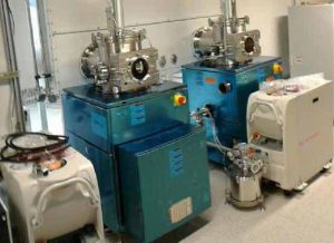
The long answer is I primarily work on developing processes for atomic layer deposition, pulsed chemical vapor deposition, and electroplating. I also train users and perform maintenance on those tools, in addition to taking care of an assortment of characterization tools, annealing furnaces, and (recently) chemical mechanical polishing. This toolset largely encompasses two microelectronics related process integration projects undertaken with the aim of expanding the breadth of services offered by the lab. One project involves through-silicon-vias, leaning heavily on conformal coatings and electroplating. A second project involves a copper damascene process which leans heavily on electroplating and chemical mechanical polishing to form two interconnected copper levels embedded in an insulating oxide layer.
WNF: What is your background? What were you working on before you came to WNF?
FN: My background is in electrical engineering. As an undergrad I became interested in semiconductor materials, and I gravitated towards microelectronic and optoelectronic device fabrication and materials characterization for my graduate studies. Prior to joining WNF, I was involved in product development and government sponsored research of III-V multijunction photovoltaics for space and terrestrial applications. For example, I managed a research project at Soitec to demonstrate a high efficiency 4-junction direct wafer bonded solar cell intended for terrestrial power generation. While in industry I had the opportunity to work in many different areas including device design, epitaxy, fabrication, and characterization. Individuals working in a single technical area were often specialists with limited knowledge of what the other areas did, or how actions taken by other areas might affect their results. I found that understanding those interrelationships was always a big part of making sense of device characteristics or running a project, which is how I became interested in process integration.
WNF: In your opinion, what makes WNF unique?
FN: WNF has a great mix of academic and industrial users. Compared to a lot of labs which focus on serving primarily one or the other, we are challenged to strike a balance between flexibility and consistency. This environment provides a lot of opportunities to meet the needs of both.
What is your favorite thing about working at WNF?
FN: I enjoy working with my colleagues here, as well as with the mix of people from technologically diverse areas. I appreciate the opportunities that this affords to improve and optimize operations from a service and efficiency standpoint, while at the same time leaving room to investigate interesting topics, demonstrate new capabilities, and develop new processes.